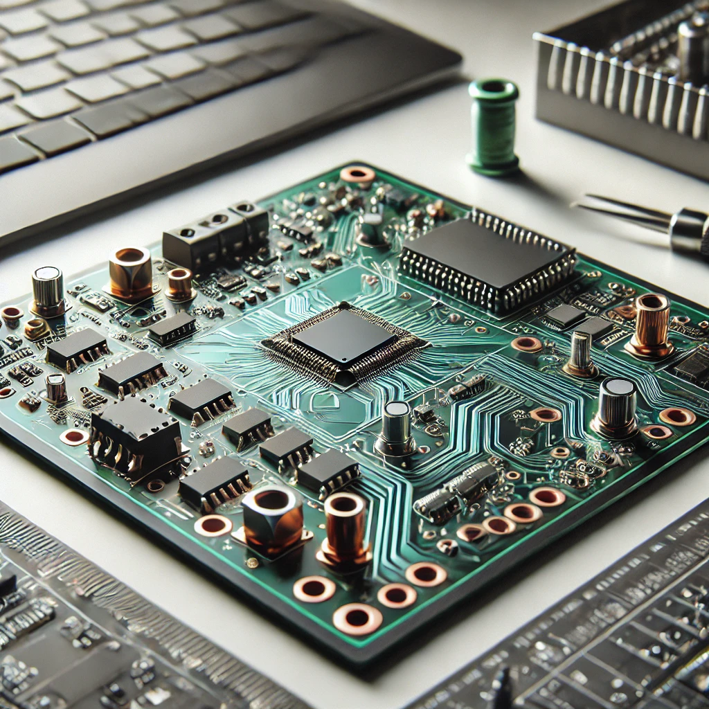
Nearly all electronic products you use every day—like phones, laptops, and drones—rely on PCBs (Printed Circuit Boards). If you’ve ever wondered how these devices work, understanding PCBs is a great starting point.
What is a PCB? Think of a PCB as the wiring system inside a device. It connects various electronic components together in a circuit. A PCB is made up of multiple layers, including conductive and insulating layers. The conductive layers, usually made of copper, have patterns of thin lines called traces. These traces act like flat wires, creating the pathways that allow electricity to flow between components. These patterns are etched onto or between layers of a non-conductive material, ensuring everything stays connected properly.
How Components Are Attached: Soldering
Once the PCB is ready, the next step is attaching electronic components. This is done through a process called soldering. Soldering not only secures the components in place but also establishes the necessary electrical connections with the board.
There are two common techniques used in PCB assembly:
- Through-Hole Soldering: Here, components have leads or wires that are inserted into holes drilled through the PCB. These leads are then soldered to pads on the opposite side of the board, creating a strong connection. This method is often used for components that need to handle mechanical stress or high currents.
- Surface-Mount Technology (SMT): In this method, components are placed directly onto the surface of the PCB. Their small metal leads or pads make contact with corresponding pads on the board and are soldered in place, usually using reflow soldering techniques. SMT allows for smaller, more compact designs and is ideal for high-speed, automated assembly.
Creating the Circuit Patterns: Etching
To create the patterns or traces on the copper layer, a process called etching is used. Here’s how it works: The copper layer is coated with a photoresist material, which can either become soluble or insoluble when exposed to light, depending on the type of photoresist used. A mask is used to selectively expose parts of the photoresist to light, protecting certain areas. After exposure, the soluble areas are washed away, leaving behind the desired pattern on the copper. The exposed copper is then etched away, leaving only the traces that form the electrical pathways on the board.
Laminates: The Backbone of PCBs
The materials used to make the layers of a PCB are called laminates. These are created by pressing layers of cloth or paper with resin under heat and pressure. Laminates can be quite large—up to 4 by 8 feet. The weave of the cloth, thickness, and resin amount are carefully adjusted to achieve the desired properties, like fire resistance and insulation.
The laminate also serves as the insulating layer, preventing electrical signals from shorting between copper traces. Common laminate types include FR-4 and CEM-1, each offering specific characteristics like strength, thermal stability, and insulation.
Substrate Materials and Their Importance
PCBs are typically made from composite materials that combine a matrix (often epoxy resin) with reinforcement (like woven or nonwoven glass fibers). The type of reinforcement used affects the material’s cost and suitability for high-frequency applications. Woven materials are cheaper but might not be ideal for high-frequency circuits, while nonwoven materials are more expensive but offer better performance.
Key characteristics of these substrates include:
- Thermal Properties: How the material handles heat, particularly the glass transition temperature (Tg), where the material softens and expands.
- Electrical Properties: How well the board insulates electricity and its dielectric constant.
- Moisture Absorption: How much water the material absorbs, which can impact performance.
FR-4 is the most common material because it offers good insulation and low water absorption. Other materials, like aluminum or flexible substrates, are used for specific needs, such as cooling or flexibility in design.
The Role of Copper Thickness
The thickness of the copper layer on a PCB is crucial for conducting electricity and dissipating heat. In the U.S., copper thickness is usually described in ounces per square foot, with common values being 1/2 oz, 1 oz, 2 oz, and 3 oz per square foot. These correspond to thicknesses of 17.05 μm, 34.1 μm, 68.2 μm, and 102.3 μm, respectively. Thicker copper layers are used for high-current or high-power applications.
Designing and Manufacturing PCBs
PCB Design
Designing a PCB starts with specialized software. You’ll capture the circuit schematic, determine the board’s size, and place components, considering factors like heat dissipation and signal integrity. The final design is exported as fabrication data, including Gerber and drill files, which guide the manufacturing process.
Panelization and Depaneling
For efficient manufacturing, multiple PCBs are often grouped on a single panel. After assembly, the panel is separated into individual boards through depaneling, which can be done with lasers or milling.
Copper Patterning and Etching
Copper traces on a PCB are created by applying a protective mask, then etching away unwanted copper. This can be done through methods like photoengraving, silk screen printing, or laser etching. The choice of method depends on the volume of boards being produced and the required precision.
Lamination, Drilling, and Vias
Multi-layer PCBs are made by stacking and laminating several layers of material, each with etched copper traces. Holes, or vias, are drilled into the PCB to connect different layers or insert components. Micro vias, used in high-density designs, are often created with lasers.
Plating, Coating, and Solder Resist
PCBs are often plated with materials like solder, tin, or gold to protect the copper and improve solderability. A solder resist, typically green, is applied to protect the board from corrosion and prevent solder from bridging between traces. A legend or silkscreen is printed on the board to indicate component locations and other important information.
Assembly and Testing
Once the PCB is ready, it’s populated with electronic components using through-hole or surface-mount technology. After assembly, the board undergoes various tests to ensure it functions correctly. JTAG boundary scan testing may also be used to check connections without physical probes.
Protection and Packaging
For harsh environments, PCBs may receive a conformal coating to protect against corrosion and moisture. Assembled boards are often placed in antistatic bags to prevent damage from static electricity during handling and transport.
Conclusion
Creating printed circuit boards (PCBs) involves a detailed and multi-step process that includes design, manufacturing, assembly, and testing. Each step is crucial to ensuring the PCB functions reliably in the final product. By understanding the intricacies of PCB production, from soldering techniques to laminate properties, you gain a deeper appreciation for these essential components that power the technology around us. As technology advances, the methods used in PCB manufacturing will continue to evolve, leading to even more sophisticated and efficient electronic devices.


